Newsletter Subscribe
Enter your email address below and subscribe to our newsletter
[forminator_form id="25163"]

All voices matter
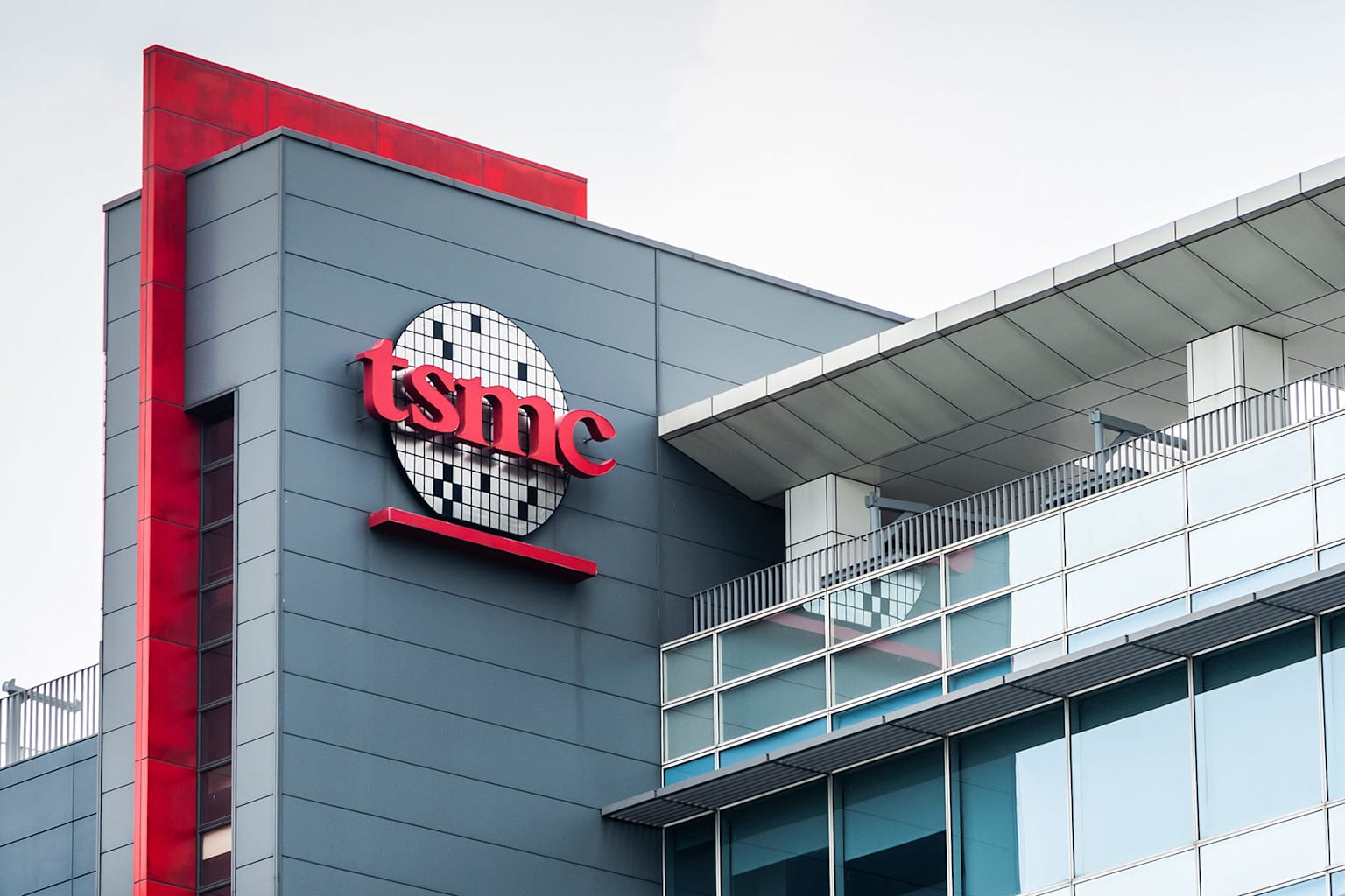
finance.yahookucoinrtiTSMC Taiwan Semiconductor Manufacturing Company Limited is building momentum for its next-generation A14 1.4-nanometer chip manufacturing process, with strong customer engagement already underway well before volume production begins in 2028. The company disclosed during its second-quarter 2026 earnings call that customer tape-outs are running ahead of schedule across both smartphone and high-performance computing applications.finance.yahoo+1
The A14 process, TSMC's second-generation nanosheet transistor technology, is designed to deliver 10% to 15% higher performance at the same power or 25% to 30% lower power at the same speed compared with its 2-nanometer N2 technology, along with nearly 20% higher chip density. Internal testing has shown encouraging results: a product-like vehicle has demonstrated close to 90% device performance, while a 256-megabit SRAM achieved nearly 90% yield.finance.yahoo
Major customers lined up for the A14 node include Apple , Nvidia , AMD Advanced Micro Devices, Inc. , Qualcomm , MediaTek, Broadcom , and several cloud service providers. Socionext announced plans to tape out a multi-core datacenter chip on A14 in September 2026, while Cadence has locked in tool certification for the process.kucoin+2
TSMC's construction of A14 fabrication plants at the Central Science Park in Taichung is progressing on schedule. The first factory is expected to be completed by April 2027, with equipment installation and pilot production to follow. A second plant is advancing in parallel, with mass production targeted for late 2027. All four planned A14 fabs are projected to be fully operational by the second quarter of 2028, with estimated monthly capacity of 120,000 to 160,000 twelve-inch wafers.techpowerup+1
TSMC also introduced A13 and A12 as derivative technologies within the A14 family. A13 is designed for more than 6% die area savings through a 97% optical shrink, while A12 will bring backside power rail technology to the platform. Both are slated for volume production in 2029.finance.yahoo
Liu Pei-chen, a researcher at the Taiwan Institute of Economic Research, noted that real yield rates, transistor performance, customer ecosystem strength, and advanced packaging integration will ultimately determine competitiveness at the 1.4nm node — not production timelines alone. Intel plans to launch its competing 14A process in 2028, while Samsung expects to commercialize corresponding technology in 2029. Liu cautioned that there is often a considerable gap between lab-stage specifications and actual mass-production cost and volume.rti+1